1296 MHz PA
with Mitsubishi RA18H1213G
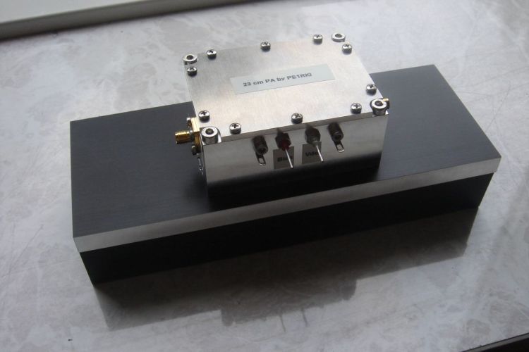
Figure 1.The finished 23 cm PA.
| This page describes how I assembled a 23 cm PA kit based on the Mitsubishi RA18H1213G power module. All components except the power module were purchased from Bert Modderman PE1RKI. He is a wizard with his CNC milling machine. Mechanical parts sold by him are beautiful and perfect! |
Circuit diagram
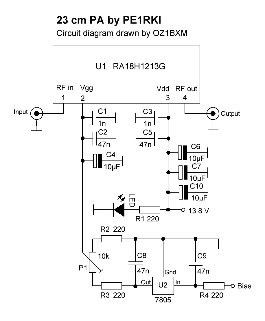
Fig. 2. Circuit Diagram.
Some component values in the kit (delivered by PE1RKI) were diffent from the circuit diagram:
| Component | Circuit Diagram | Delivered with kit |
| C2, C5, C8, C9 | 47 nF | 6n5 SMD |
| C4, C6, C7, C10 | 10 µF | 22 µF SMD |
| R1, R2, R3, R4 | 220 ohm | 240 ohm SMD |
Photos
Click any image to enlarge. Hit "Back" to return here.
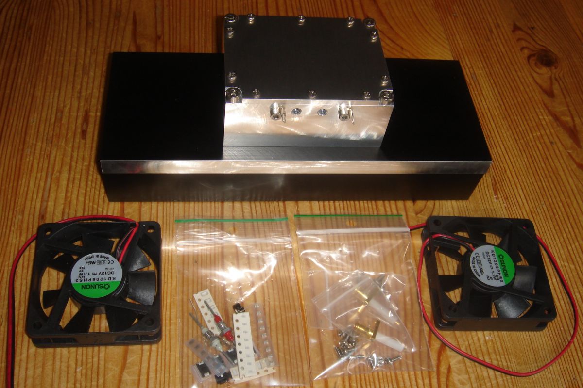
Figure 3. Kit from PE1RKI.
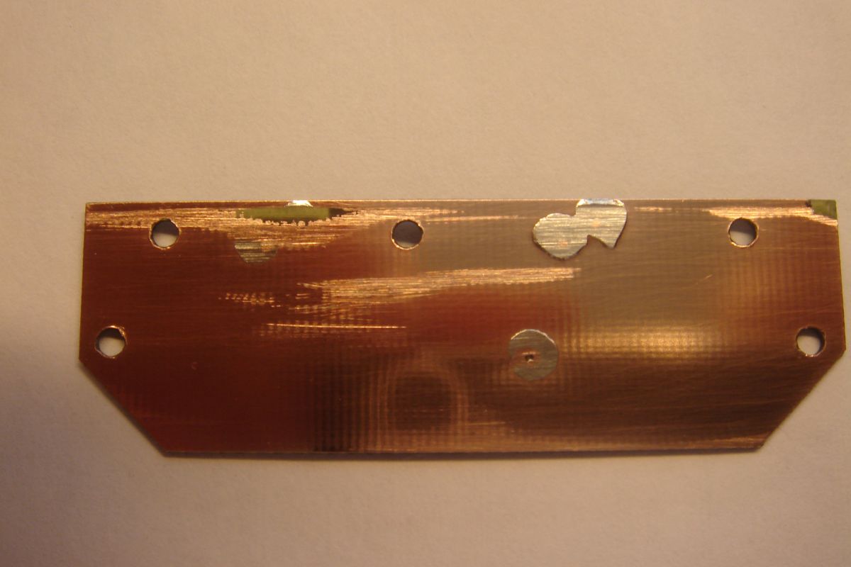
Figure 4. Bottom side of PCB. The
delivered PCB did not have plated-through holes (plated-through holes connect
top side tracks with bottom side tracks). I soldered 5 wire
bridges and made the bottom side smooth using a file. As you
can see, some of the wire bridges are inferior (my fault - too
much filing). Lastly, the PCB bottom side was thoroughly
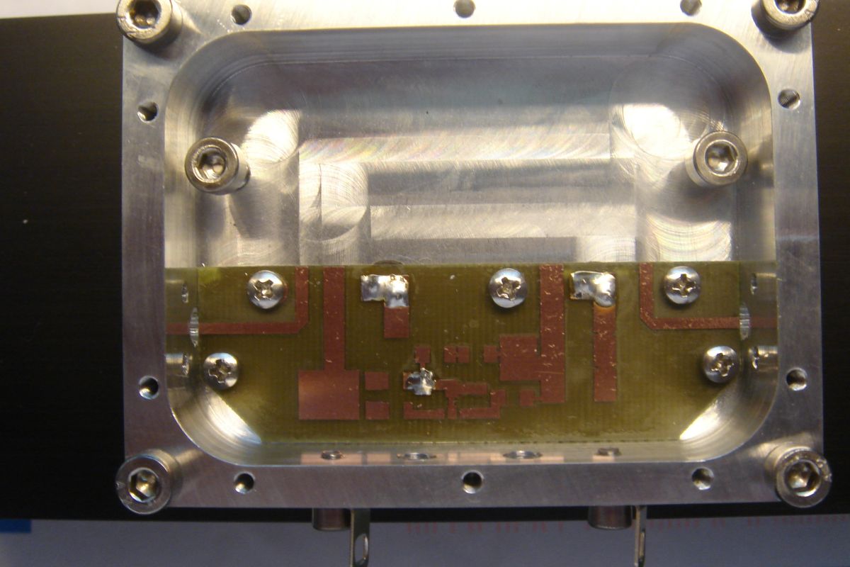
cleaned. 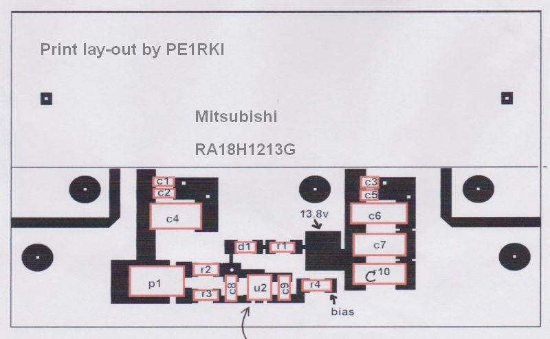 Figure 5. Print lay-out. Figure. 6. The PCB is fastened with 5 screws. There was an error on the PCB. I had to cut a copper track. It is
marked in the picture above. Click the picture for a better view. I checked the connection between the metal house and the 3 ground connected tracks. The diode tester showed 0.00 volt, which indicates a perfect connection with no voltage drop. The PCB stays in the house during soldering of the remaining components.  Figure 7. Sanding the bottom side of the power module. To
make the bottom side of the power module smooth, I first
removed the two metal protrusions with a file. Then
followed sanding to further smooth out the surface. |
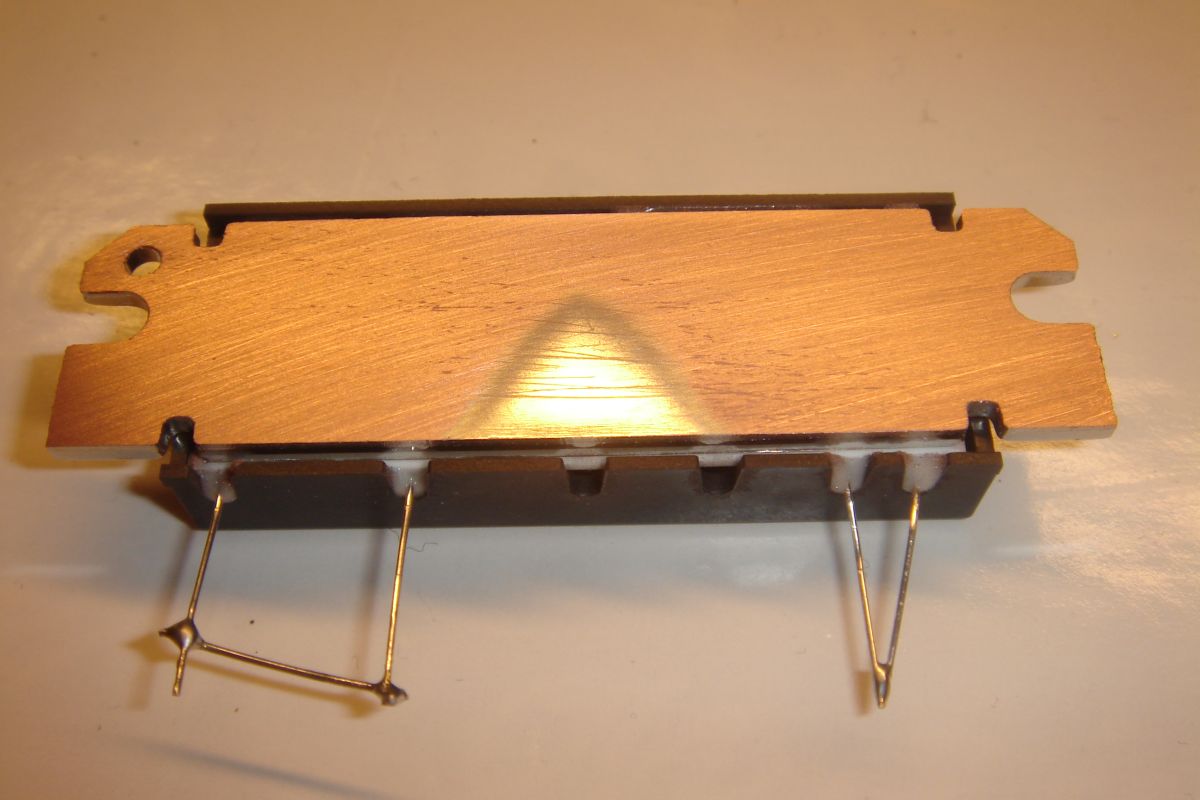 Figure 8. Bottom side of the power module. The
picture shows the bottom side of the power module, which is ready
for fitting into the metal house. Input and output wires
were soldered to ground to prevent ESD during sanding. 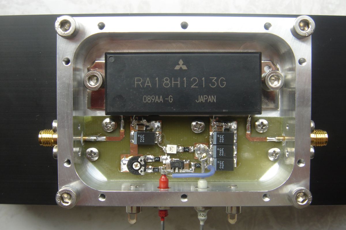 Figure 9. All components soldered. The
RA18H1213G module is mounted without any thermal compound. A solid RF
ground is more important than slightly improved heat transfer. I have added a short piece of wire between the cathode of D1 and the leftmost ground track. This wire is optional. The input connector (sma female) is seen to the left; the output connector is to the right. The grey feed-through capacitor carries Vdd and the red one enables bias (apply +12 V). The bias voltage Vgg is set with the black trimpot. 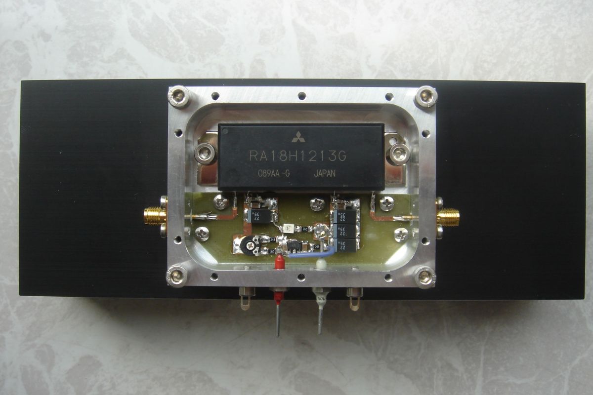 Fig. 10. The black heat sink measures 200 mm x 75 mm. The
metal house is fastened to the heat sink by 4 screws in the corner. A
thin layer of "Arctic Silver 5" is applied between the metal
house and the heat sink in order to enhance heat transfer. 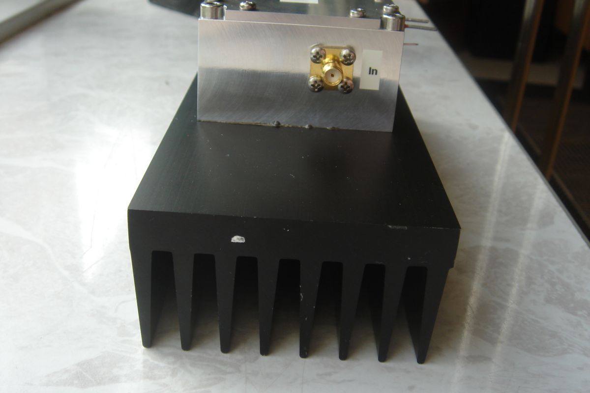 Figure 11. The heat sink is 40 mm high. |
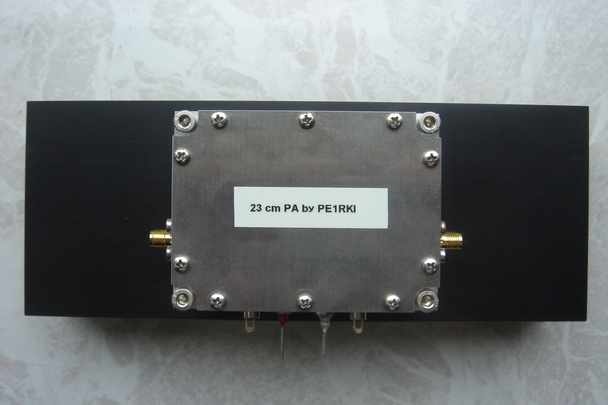 Figure 12. The finished PA (bottom side). |
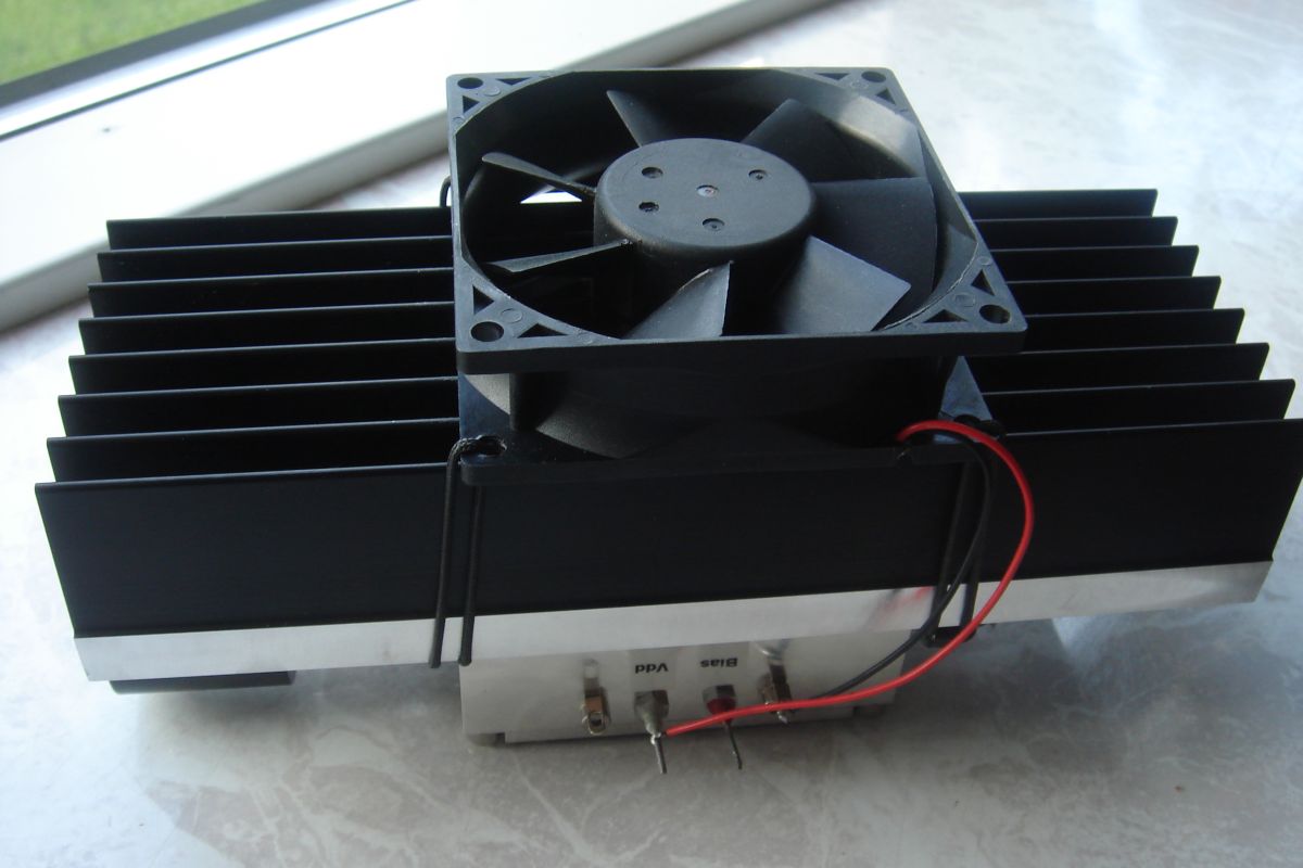 Figure 13. The finished PA (top side). I
did not use the two small fans included with the kit. The 80 mm
fan in the picture is powerfull and
almost noiseless. The air is blown from above onto the heat sink and distributed between
the fins. |

Measuring output power
- Frequency was 1296.1 MHz
- Supply voltage (Vdd) was 13.56 V DC
- Pout was measured with Bird 43 power meter (Bird 50E plug) and a 25 W dummy load
- Pout was passed through a low-pass filter having 0.25 dB attenuation at 1296 MHz
| Pin | Pout | Bias Current | Total Current |
| 300 mW | 23 W | 3.5 A | 8.2 A |
| 400 mW | 23 W | 3.5 A | 8.4 A |
| 100 mW | 15 W | 1.0 A | 5.2 A |
| 200 mW | 20 W | 1.0 A | 6.4 A |
| 300 mW | 21 W | 1.0 A | 6.7 A |
| 100 mW | 5 W | 0.4 A | 2.9 A |
| 200 mW | 17 W | 0.4 A | 5.2 A |
| 300 mW | 19 W | 0.4 A | 5.9 A |
Figure 14.
Photo from the lab during measurements. Click to enlarge.
Written by OZ1BXM
Lars Petersen. Latest revision 06-Feb-2017.