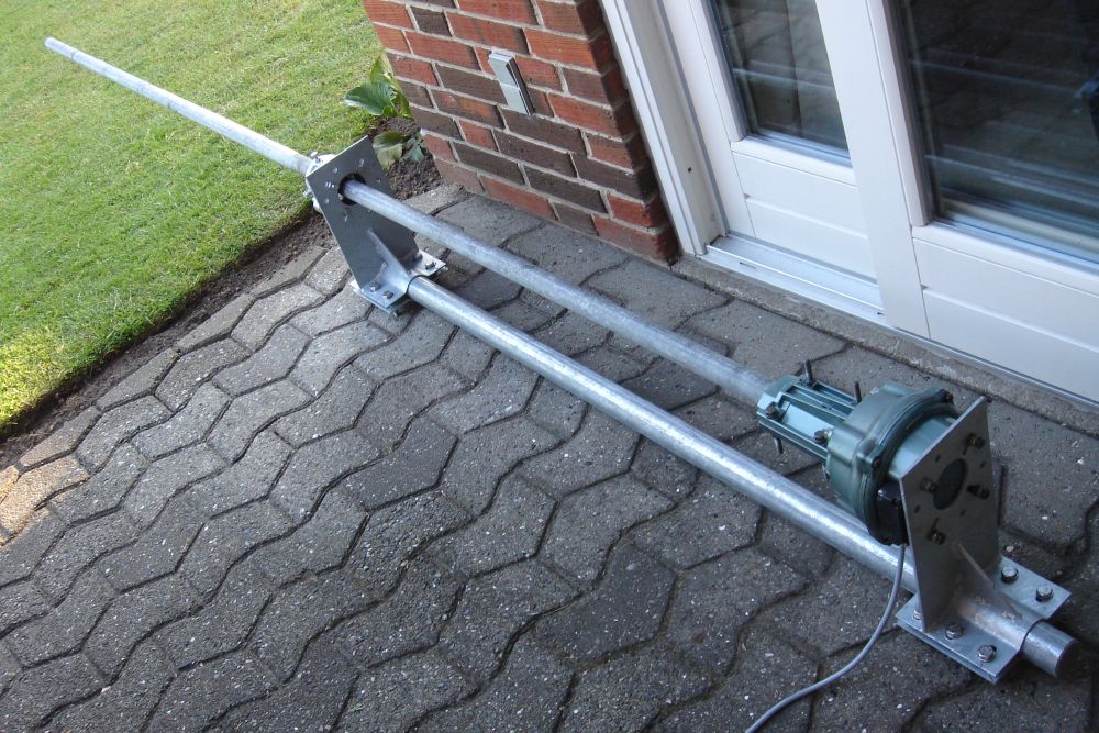
Rock-stable LNB with GPSDO
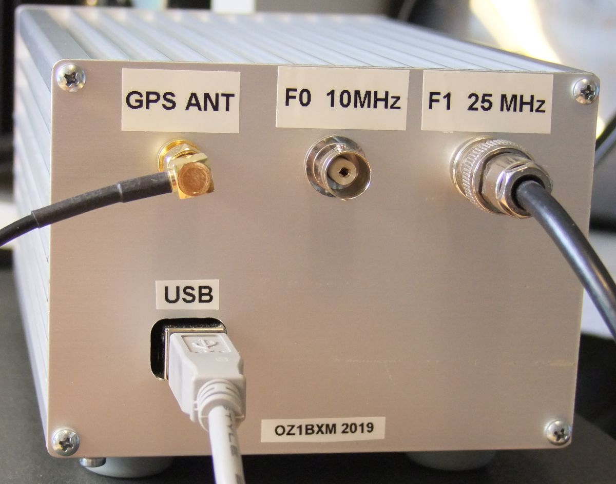
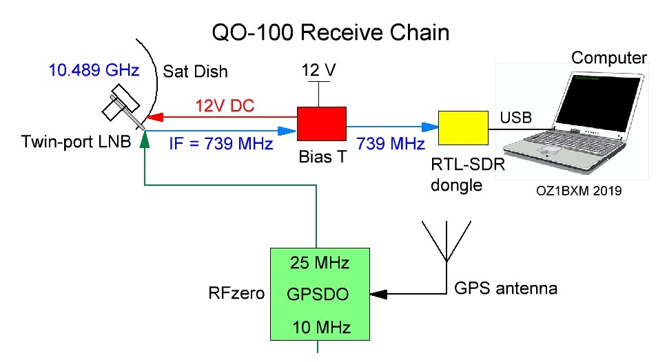 QO-100 Receive chain with GPSDO. | Block diagram A consumer type LNB for Ku-band can be used for receiving the QO-100 satellite transponder. A LNB with PLL-oscillator has an acceptable frequency stability after warm-up, but it still drifts. The reason is outdoor temperature changes and a simple oscillator using a cheap crystal. Adding a GPSDO greatly improves the frequency stability in the receive chain. The block diagram shows how the GPSDO injects a clock signal into the LNB. My GPSDO was developed by the RFzero project. The twin-port LNB is modified to accept an external 25 MHz signal via one of the ports. The LNB mod described here is not overly difficult, but you'll need accuracy and patience! |
LNB modification | |
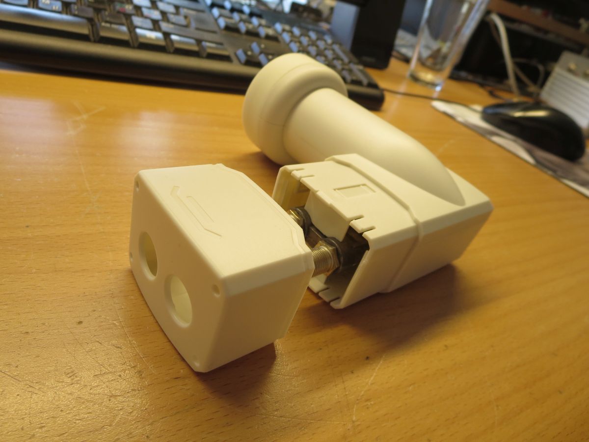
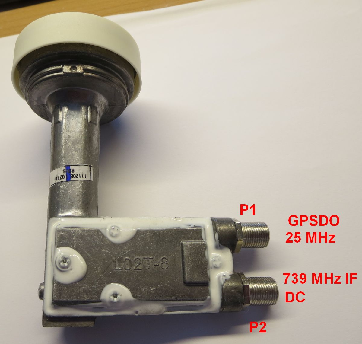 Twin-port LNB (Maximum ST-12). | Twin port LNB (Maximum ST-12) This LNB was purchased in a local home improvement store (Harald Nyborg). P1 receives the 25 MHz clock signal coming from the GPSDO. Why feed 25 MHz into the LNB? Because this frequency replaces the signal generated by the crystal oscillator. The 25 MHz clock is multiplied by factor 390 inside the LNB to provide LO at 9.75 GHz. P2 serves as IF output at 739 MHz. A DC voltage of 12 V is also applied to P2 and it powers the LNB. |
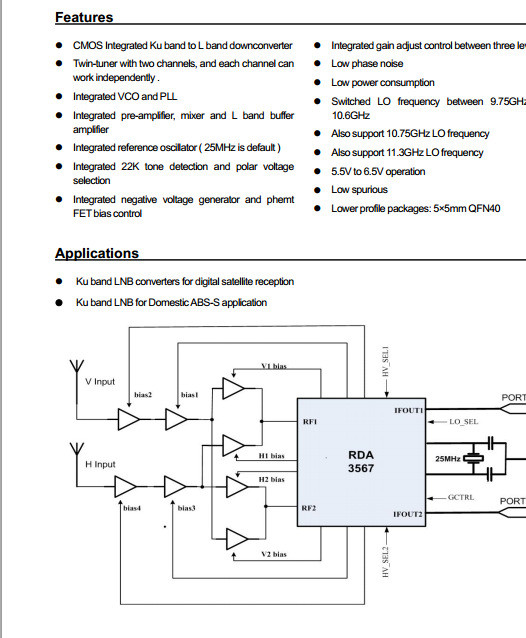 RDA3567 overview. | RDA3567 The LNB employs the RDA3567. It's a down-converter chip with 2 independent channels. It has a crystal oscillator which generates the 25 MHz clock signal. The LO at 9.75 GHz is phase locked to the 25 MHz frequency (PLL). The picture to the left was tweeted by @uhf_satcom on March 13, 2019. |
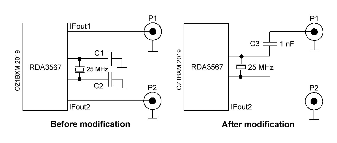 Modification overview (click to enlarge). | Modification overview The LNB modification is shown in the diagram. C1 and C2 are removed. This will disable the 25 MHz crystal oscillator. A 25 MHz square wave from the GPSDO is applied to P1. The 25 MHz signal is transferred to one of the RDA3567 clock pins via a 1 nF capacitor. |
 Removing the cable cover. | Remove the cable cover The cable cover can easily be removed. |
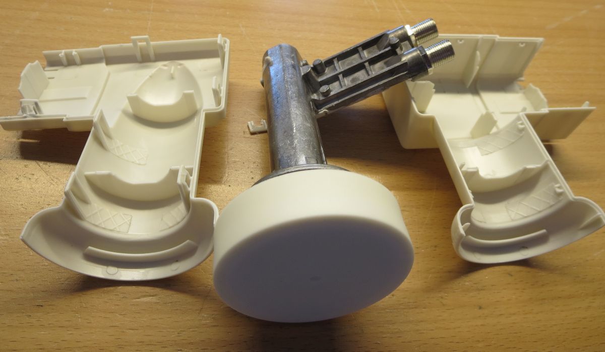 Removing the plastic house. | Remove the plastic house The plastic house is removed by releasing the clips one by one. Use a screw-driver for releasing the clips. Careful, don't break the clips! |
 The metal lid is ready for removal. | Remove the metal lid Next task is to remove the metal lid (it is secured by 4 screws). All screws must be removed before the lid can be lifted. Do not push the lid sidewards; lift it up vertically. The white sealant should be removed as necessary. 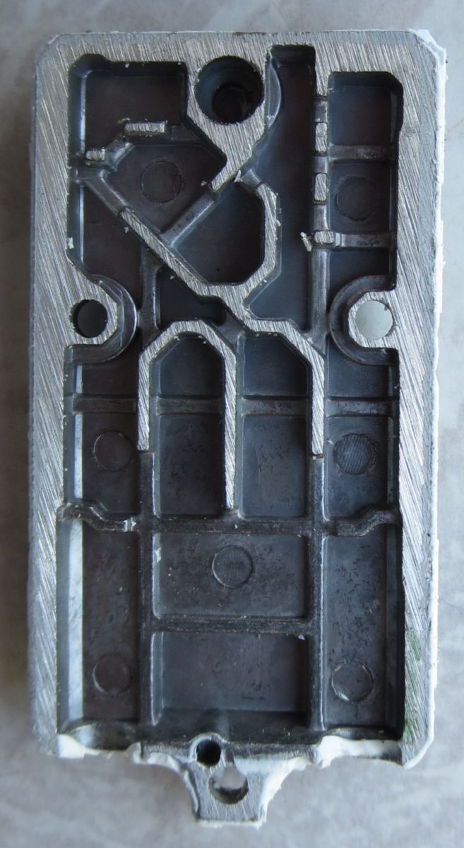 The removed lid. |
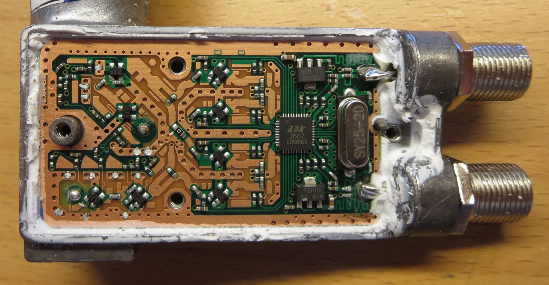 The unmodified PCB - click to enlarge. | The unmodified PCB |
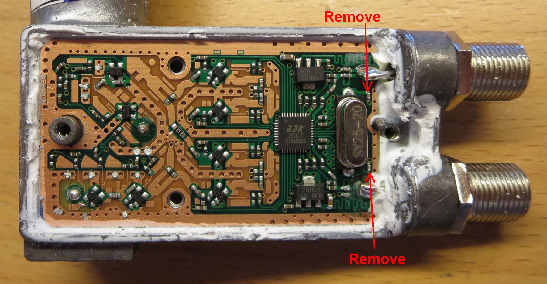 C1 and C2 before removal - click to enlarge. | Remove C1 and C2 Remove the two small capacitors. |
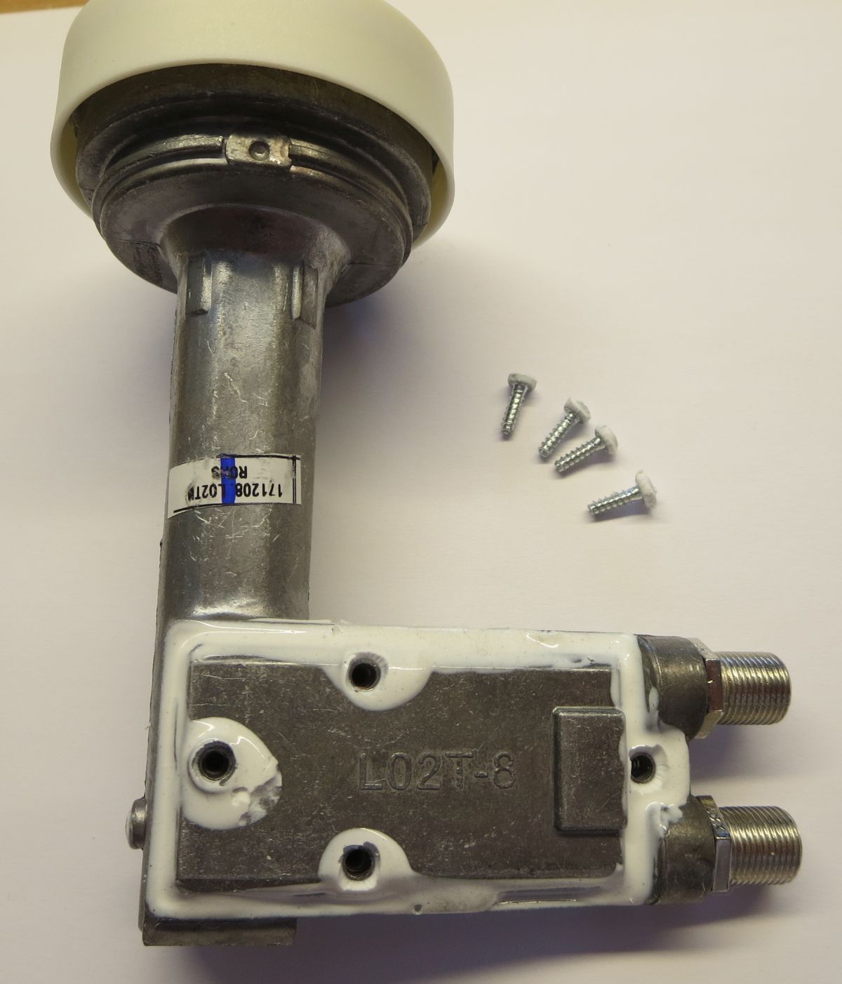
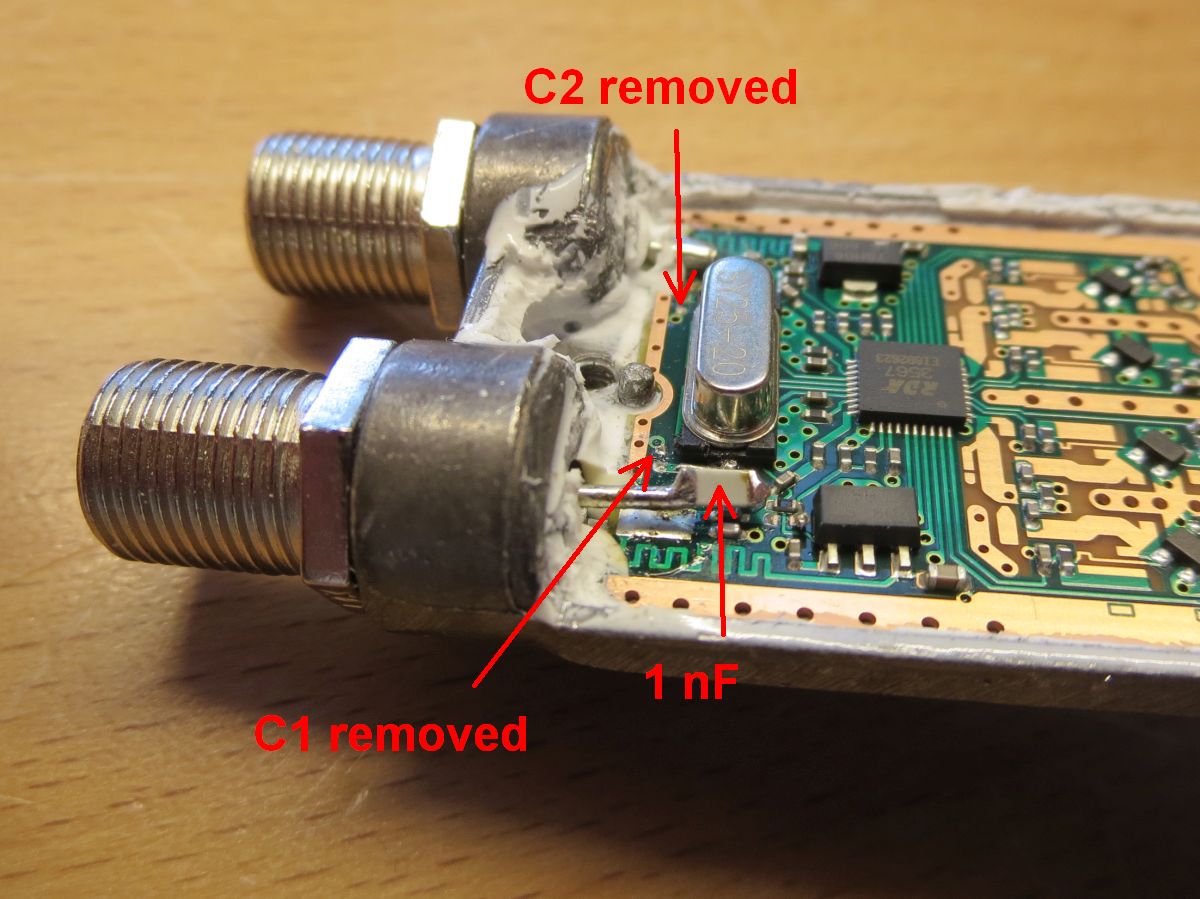 A 1 nF capacitor was added - click to enlarge. | Disconnect pin, add capacitor The center pin of P2 must not connect to the PCB track. Tin on the P2 pin is sucked away using desoldering braid. The center pin is now free. The new 1 nF capacitor C3 is connected between the center pin of P2 and the nearest crystal pin. I've added a short wire between the crystal pin and the new capacitor (1206 SMD capacitor, see picture). The other end of the capacitor was soldered directly to the P2 center pin Mount the metal lid Finally, the lid was mounted and sealed. |
GPSDO
|
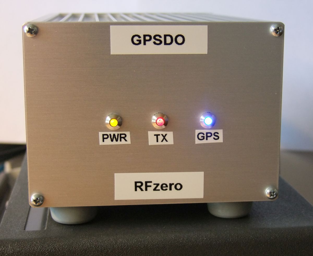
GPSDO front view. |
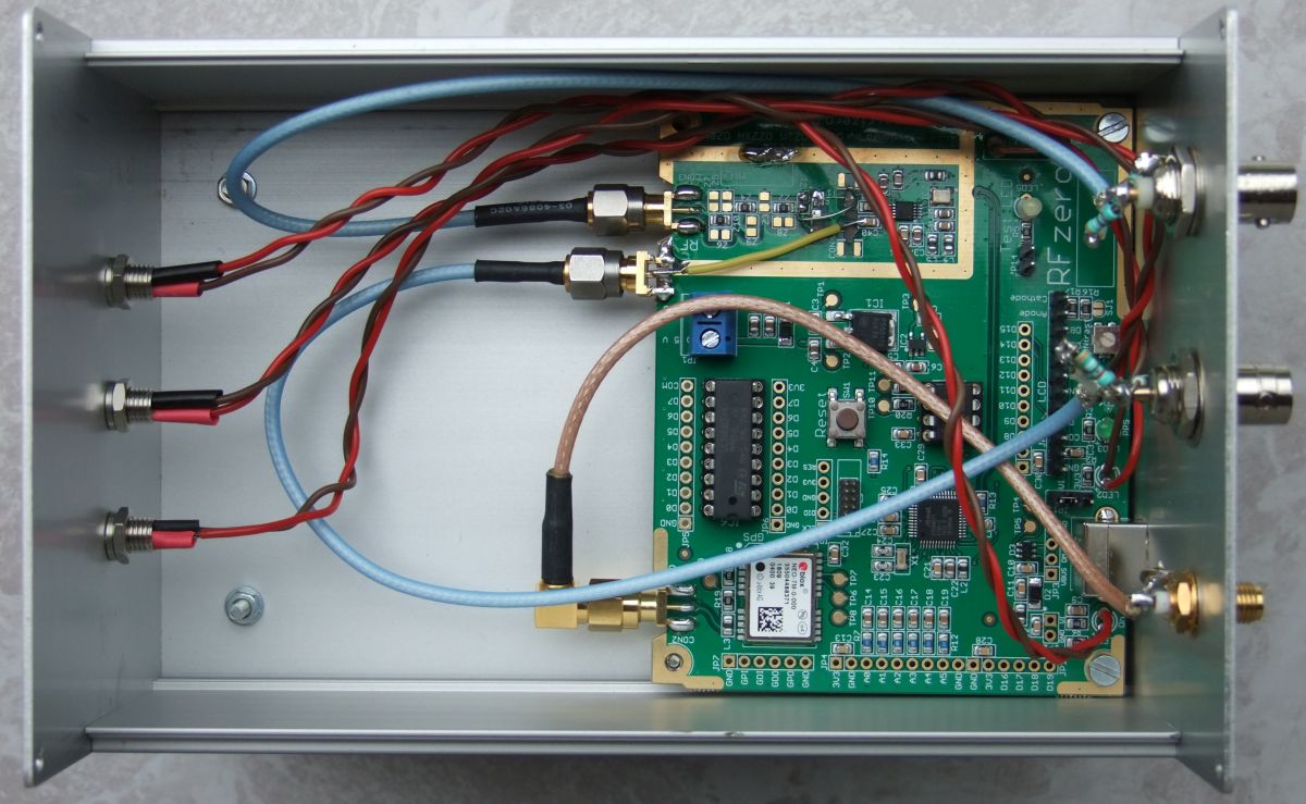
GPSDO hardware is RFzero The GPSDO hardware is the RFzero board, which is built into a metal cabinet. The RFzero board was purchased from the RFzero project by 5Q7J, OZ2XH, OZ5N and OZ2M.RFzero is a GPS-controlled clock oscillator board. RFzero is programable via Arduino IDE. The development procedure is exactly the same as when creating and uploading Arduino sketches. The RFzero project offers example files to get you started.
The alu-box is a Proma 130044 measuring 165 mm x 114 mm x 80 mm.
|
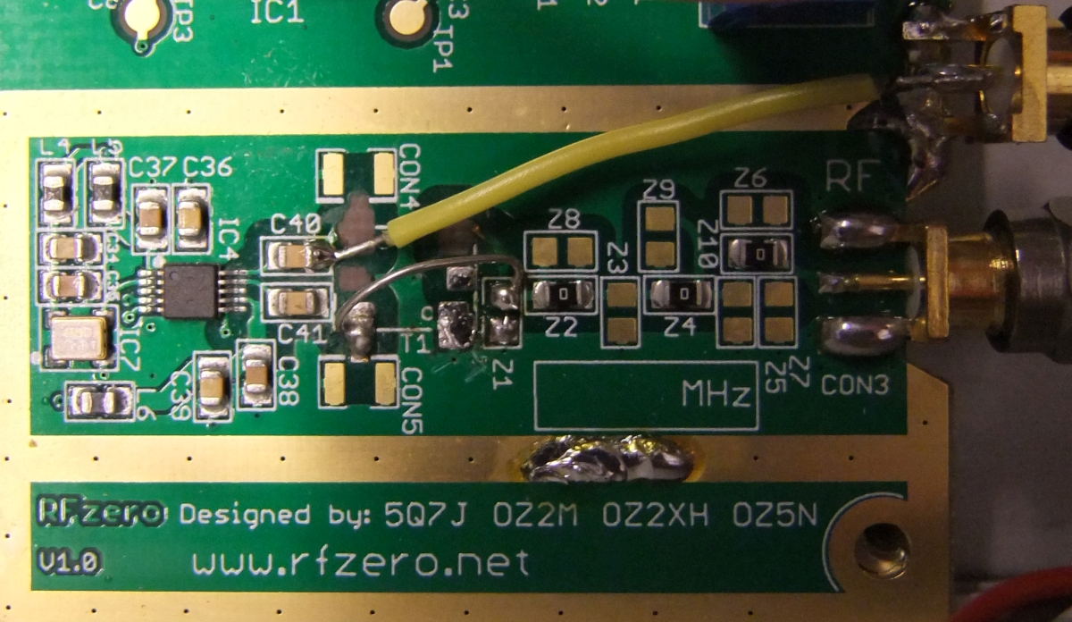 HW modifications. | RFzero HW modifications T1 is a transformer which combines two outputs from IC4. The combined signal pass the filter section and is available as RF output on CON3. The filter section is not configured from the factory (there are 3 zero-ohm resistors, and signals pass through the filter unchanged).
Click the picture to enlarge. In step 4, I soldered the jumper to one of the T1 terminals instead of C41. The result is the same. |
|
GPSDO with cover removed. |
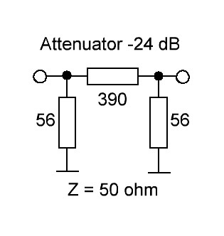
Output attenuator
|
 GPSDO rear view. | Configuration of RFzero Setting up RFzero as a clock generator for a Qatar Oscar 100 ground station is described here. Preconditions: RFzero is connected to your PC via a USB-cable. The RS232 connection is up and running (9600-8-N-1). The RFzero library is v.0.8.5. QO100.ino version 0.9.1 was compiled and uploaded to the RFzero board. Open the Serial Monitor in Arduino IDE and type the following: RFzero>config RFzero config>wr f0 10000000.000 1 RFzero config>wr f1rx 25000000.000 1 RFzero config>wr f1tx 25000000.000 1 RFzero config>rd cfg RFzero config>exit |
Written by OZ1BXM
Lars Petersen 10-June-2019. Revised 17-Jan-2020.